Signal integrity check by simulation to improve PCB performance Circuit Diagram Understanding signal integrity basics is important for anyone involved in PCB design. Signal integrity refers to the quality of an electrical signal as it travels through a circuit, impacting whether it reaches its destination without degradation. For those new to the concept, signal integrity issues can lead to various operational problems Signal integrity directly affects the performance and reliability of electronic systems, making it a critical consideration in printed circuit board (PCB) design. In PCB design, signal integrity ensures that electrical signals reach their destinations without distortion, noise, or timing issues that can compromise functionality.

In high-speed printed circuit board (PCB) design, ensuring signal integrity is crucial to achieve reliable and efficient performance. Signal integrity refers to the preservation of the quality of electrical signals as they travel through the PCB, free from distortion and noise. Several factors influence signal integrity, including via design, ground plane strategies, and design for
Enhancing Signal Integrity in PCB Design: Key Considerations and ... Circuit Diagram
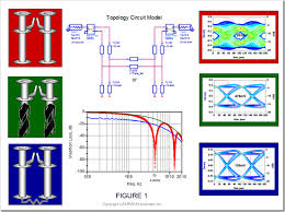
Avoiding signal integrity issues in a PCB is extremely complex for designers. It requires a deep understanding of signal integrity design rules and techniques. With the introduction of faster logic families, the designers have realized that simple PCB layouts cannot survive the signal integrity requirements. This likely describes most our the traces you would already find on a PCB, however, in order to turn a trace into a high-frequency carrying microstrip, we need to design it to have a 50 Ohm impedance. There do exist other high-frequency PCB structures that can be configured to a particular impedance such as: Stripline; Coplanar Waveguide Maintaining signal integrity in high-speed PCB design requires an integrated approach that addresses via design, ground plane strategies, and DFM. By comprehending the influence of each component and implementing best practices, designers can create dedicated and high-performance PCBs that fulfil the demands of modern electronic applications.

Many of the PCB layout and routing guidelines in use today, even for moderate speed signals and devices, are meant to ensure signal integrity. If you're new to PCB design and you've never experienced signal integrity problems, the concept of ensuring signal integrity in a design might seem esoteric. Modern PCBs can experience many problems Optimizing signal integrity in PCB design is a critical aspect of ensuring the reliable performance of high-speed electronic systems. By addressing issues such as noise, crosstalk, reflection, and EMI, and implementing strategies such as differential pair routing, grounding techniques, and impedance matching, designers can significantly improve
9 factors that lead to signal integrity issues in a PCB Circuit Diagram
In high-speed PCB design, maintaining signal integrity is critical because even minor signal distortions can lead to data corruption, communication errors, and overall system failure. Basics of Signal Integrity Signal integrity refers to the quality and reliability of electrical signals as they travel through a PCB (Printed Circuit Board). In Impedance matching: At digital circuit frequencies, signal lines act like transmission lines, and the impedances of the source, receiver, and signal traces should be matched to minimize the reflections.PCB trace termination techniques may be used, the length of stub traces should be reduced and devices should be daisy-chained. Keep signal lines short and use wide return paths.
